A DIY Community for Tech, Science, and R&D
Join a culture of sharing, growth and collaboration. You can be a part of the maker movement!
Note the VGA as designed here will ONLY fit inside the Fipsy V2 device. The pong demo only uses about 33% for the Fipsy V2 capacity, but that’s too much for the Fipsy V1.
There are two versions of the VGA example, one that is fully based on break-out components (including many wires involved), and a slimmer version that uses a dedicated Fipsy VGA Companion Board (few wires, and different code to control the colors).
We wish to thank:
The materials you will need are:
Download the VGA example (for bare boards) – from here: https://github.com/MoCoMakers/Fipsy-FPGA-edu/tree/master/Examples/FipsyV2%20-%20XO2-1200/7.%20VGA/VGA
Open the FipsyBaseline.ldf project file in Lattice Diamond.
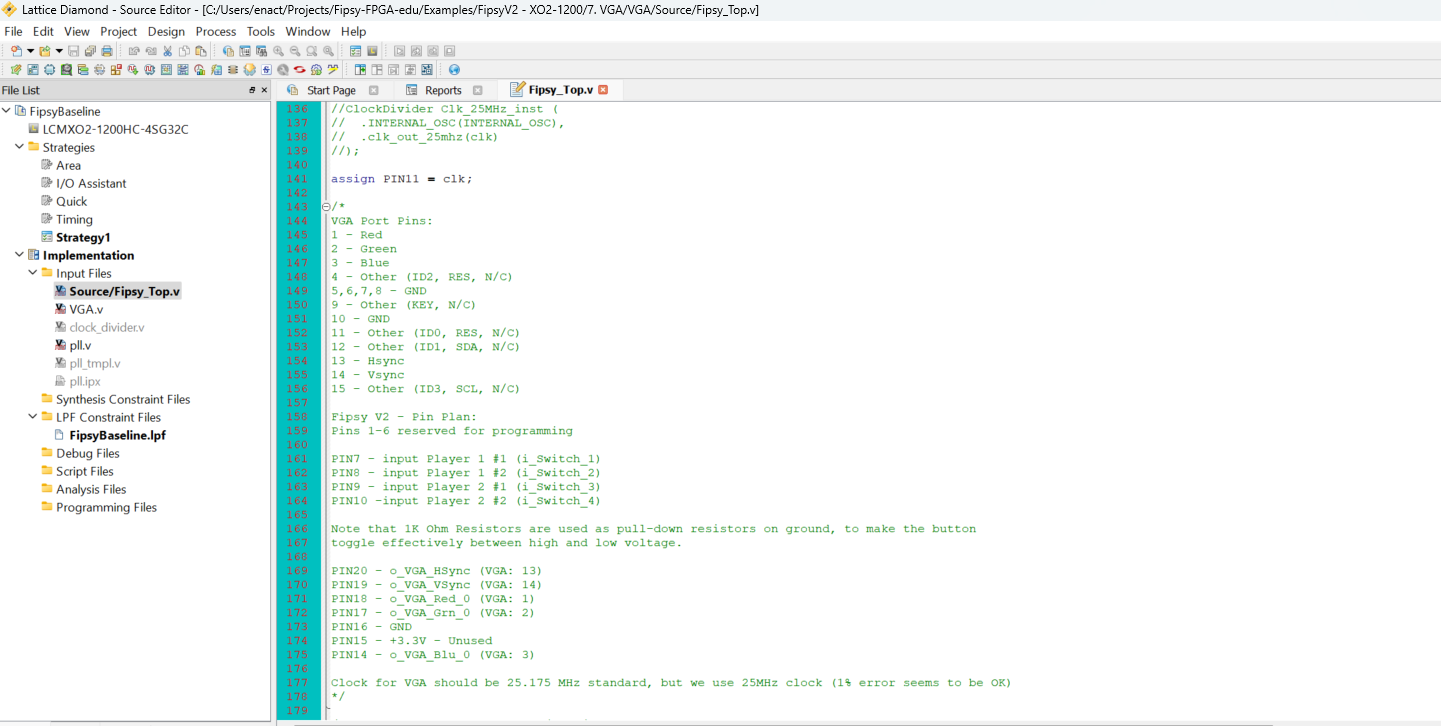
Notice how the wiring is documented in the Fipsy_Top.v file:
Once the project is uploaded on the Fipsy FPGA V2, connect the wiring. Click the image below to open a reference PDF:

Push button switches for the game pads might have connections like this, and these are assumed in the above wiring schematic:
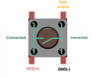
More on push button switches here.
VGA Port Pins:
1 – Red
2 – Green
3 – Blue
4 – Other (ID2, RES, N/C)
5,6,7,8 – GND
9 – Other (KEY, N/C)
10 – GND
11 – Other (ID0, RES, N/C)
12 – Other (ID1, SDA, N/C)
13 – Hsync
14 – Vsync
15 – Other (ID3, SCL, N/C)
N/C = Not Connected, as it relates to our project.
R,G, B Pins are designed to be a variable voltage between 0V and 0.7V – and this would affect brightness of that value. Our design does not account for this variable brightness, and uses an all-or-nothing voltage value.
The wiring includes two player game controllers, each with two buttons – up and down:
Fipsy V2 -> VGA
Pins 1-6 reserved for programming (can be connected to ESP32 via SPI for example)
PIN7 – input Player 1 #1 (i_Switch_1)
PIN8 – input Player 1 #2 (i_Switch_2)
PIN9 – input Player 2 #1 (i_Switch_3)
PIN10 -input Player 2 #2 (i_Switch_4)
Note that 1K Ohm Resistors are used as pull-down resistors on ground, to make the button toggle effectively between high and low voltage.
PIN20 – o_VGA_HSync (VGA: 13)
PIN19 – o_VGA_VSync (VGA: 14)
PIN18 – o_VGA_Red_0 (VGA: 1)
PIN17 – o_VGA_Grn_0 (VGA: 2)
PIN16 – GND (VGA: 5,6,7,8)
PIN15 – +3.3V – Unused
PIN14 – o_VGA_Blu_0 (VGA: 3)
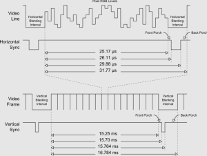
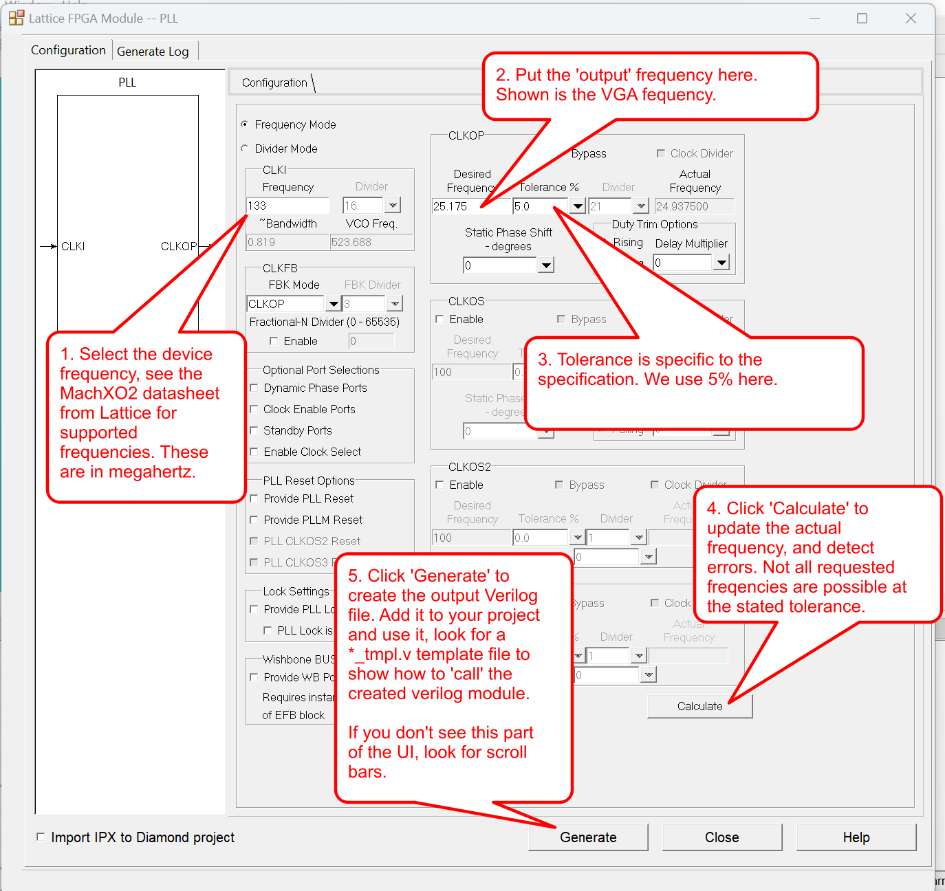
Clock for VGA should be 25.175 MHz standard, but we use 25MHz clock (1% error seems to be OK)
NOTE: For R,G, and B pins, we insert a 280 Ohm resistor to drop those lines to full brightness of 0.7V. We were able to test the design without these resistors, and the screen would still display (that is we we drove these lines at the Fipsy default of 3.3V) – but this is FAR out of specification for VGA, and it may damage your electronics. This design is not specification compliant, so use caution here as your electronics could be damaged.
Using pins such as these – https://lab.arts.ac.uk/books/physical-computing/page/how-to-connect-a-push-button-or-switch
We connect each ground on the switch buttons to GND using a 1K Ohm resistor.
See also:
http://tinyvga.com/vga-timing/640×480@60Hz
https://tomasz-cichocki.pl/posts/012-VESA-output-by-FPGA
Note that to start the game click “Up” on player 1’s controller/button. Things will now be in motion.
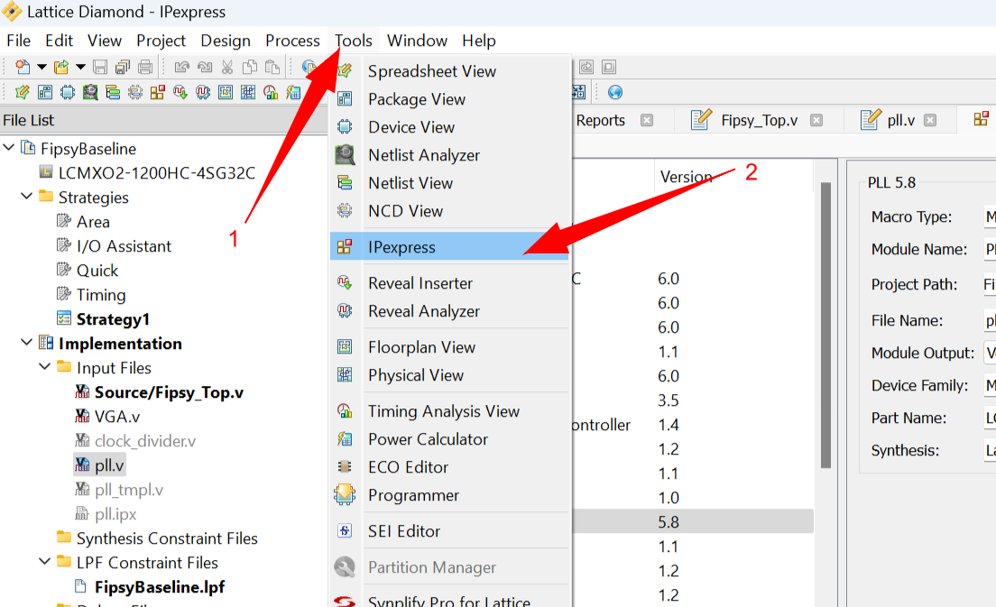
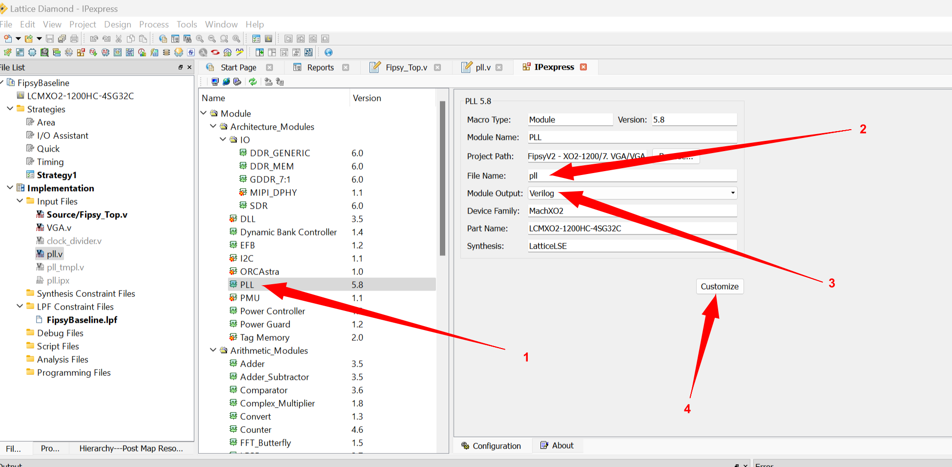
PLL, or Phase Lock Loop is a recommended way to generate new system clock frequencies.
The PLL is a module supported by the Fipsy V2 as an IP Core (but not by the Fipsy V1 – though other techniques can be used to generate custom frequencies such as registry counters).
The VGA demo uses this to create a clock line. See here:
wire clk;

pll Clk_25MHz_inst (.CLKI(INTERNAL_OSC), .CLKOP(clk));
This sets a `clk` element to our frequency (approximately 25MHz) using a PLL. See how the PLL was created here:
This companion board is in development. Check back here soon!